Beyond Semiconductor
IP   ›   Peripherals   ›   DDR2/DDR SDRAM Memory Controller    
Beyond DDR2/DDR SDRAM Memory Controller


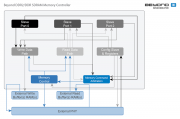
SDRAM memory evolution is going into the direction of increased latency at increased frequency. Beyond DDR2/DDR SDRAM Memory Controller IP Core was developed with this trend in mind. It interleaves accesses from multi-port front-end when possible, maximizing utilization of memory control and data buses. This utilizes higher memory bandwidth capabilities as additional latency cycles can be used for housekeeping operations – bank, row and refresh management.
Controller supports wide variety of applications with its comprehensive set of compile time and run time configuration options. Physical layer (PHY) interface is simple generic interface that can easily connect to various PHY implementations.
click to enlarge


Memory Interface
  • Compile time configurable number of chip select signals – one to four
  • Software programmable chip select address range for each chip select – 8MB to 4GB
  • Compile time configurable memory data bus width. Supported 16, 32 and 64 bits
  • Utilization of write data mask signals for partial write bursts
  • Compile time configurable memory address bus width
  • Standard DDR SDRAM control interface
  • Possible SDRAM burst sizes are 1, 4, 8 for DDR and 2, 4, 8 for SDR
  • Software programmable SDRAM memory device timings
  • Software programmable SDRAM memory organization
  • Fully configurable DDR2 SDRAM ODT control using programmable matrix
  • Independent of data transmit and capture (physical layer) implementation
  • Pipelined, out-of-order memory command generation. Number of pipeline stages is selected at compile time according to application needs
  • Automatic SDRAM refresh generation
  • Register interface for software initialization and suspension of external memory device
  • Page tracking logic implemented to reduce access latencies. Tracked number of pages is selected at compile time according to application needs
 
 
Supported SoC Bus Interconnect
  • The Memory Controller IP Core implements up to three AXI / AHB / WB SoC Bus interfaces. Increased interface count possible on request
  • Burst operations are utilized to increase memory and buses throughput. All AXI / AHB / WB burst, classic and single transfer cycles are supported
  • Read burst pre-fetch behavior configured independently for each port
  • Each memory access port can be configured at compile time to support either 32 or 64 bit data width
  • Separate AXI / AHB / WB interface is implemented for configuration space access, which keeps SoC memory map flexible. It is used to configure the core, initialize external memory devices and physical layer
 
Core Internals
  • Memory control logic can run at any integer multiple frequency of AXI / AHB / WB Interconnect frequency, including 1x.
  • Each implemented AXI / AHB / WB port can operate of its own clock source and frequency.
  • Top level buffer RAM interface supports industry standard, 1 clock latency synchronous dual port RAMs – simple integration for any technology
  • PHY interface can run on 1x or 2x memory control logic frequency – 2T timing support
  • Compile time configuration of control and data paths. Parameters enable/disable sharing of same RAM buffer resource between different AXI / AHB / WB ports, allowing various tradeoff scenarios for size and speed


Beyond DDR2/DDR SDRAM Memory Controller


If you would like to inform yourself further about Beyond Semiconductor products, please complete the webform below and let us know your questions, requirements or requests.
 
Please note that all submitted information will be handled confidentially and used only to address your inquiry. Therefore, we kindly ask you to fill out all the fields of the form.
 
You may expect our answer shortly.
 

Name (first, last):*
Corporate email address:*
Company:*
Subject:
Your inquiry:*


Copyright © 2006 - 2024 Beyond Semiconductor. All rights reserved.